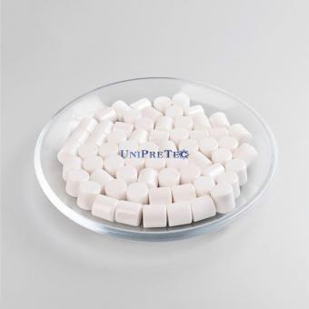
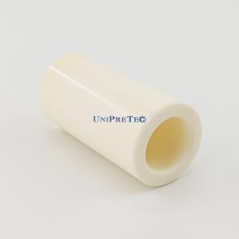
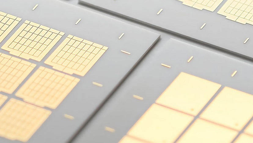
Because of the advantages of good heat dissipation, high insulation, high temperature resistance, and corrosion resistance, pcb ceramic substrates are widely used in electronic products such as automotive electronics, transportation rails, semiconductors, power modules, and LEDs. So what production process is used in the production of PCB ceramic substrates?
- Direct Plated Copper Ceramic (DPC) process DPC substrate has the advantages of high graphics accuracy and vertical interconnection, and is mainly used in high-power packaging.
- Direct Bonded Copper Ceramic (DBC) process has a thicker DBC circuit layer and better heat resistance, and is mainly used in IGBT packages with high power and large temperature changes.
- thick film printing ceramic substrate (Thick Printing Ceramic, TPC) process
TPC thick-film ceramic substrates have good heat resistance and low cost, but have poor circuit layer accuracy, and are mainly used in automotive sensors and other fields.
- thin film ceramic substrate (ThinFilm Ceramic, TFC) process
In the plane ceramic substrate, the thin film ceramic substrate TFC substrate has high pattern accuracy, but the metal layer is thin, mainly used in the packaging of small current optoelectronic devices
- AMB active brazing process
The AMB substrate has a thicker circuit layer and better heat resistance, and is mainly used in IGBT packages with high power and large temperature changes.
- multi-layer htcc high temperature co-firing process
The high-temperature co-fired ceramic materials are mainly ceramics with alumina, mullite and aluminum nitride as the main components, and no glass is added to the ceramic powder of HTCC. The conductor paste is made of tungsten, molybdenum, molybdenum, manganese and other high melting point metal heating resistor pastes. The sintering temperature is 1600°~1800°. Because HTCC substrates have the advantages of high structural strength, high thermal conductivity, good chemical stability, and high wiring density, they have broad application prospects in high-power micro-assembled circuits.
- multi-layer Itcc low temperature co-firing process
In order to ensure high sintering density under low temperature co-firing conditions, low-temperature co-fired ceramics usually add amorphous glass, crystallized glass, low-melting oxides, etc. to the components to promote sintering. Glass and ceramic composites are a typical low temperature co-fired ceramic material. In addition, there are crystallized glass, composites of crystallized glass and ceramics and liquid phase sintered ceramics. The sintering temperature is 900°~1000°. LTCC uses Au, Ag, Cu and other metals with high conductivity and low melting point as conductor materials. Due to the low dielectric constant and low loss performance of glass ceramics at high frequencies, it is very suitable for RF applications. , microwave and Manmie wave devices. Mainly used in high-frequency wireless communication, aerospace, memory, driver, filter, sensor and automotive electronics and other fields.
Summary: Among the double-sided ceramic substrates, DPC ceramic substrates have rapidly occupied an important market position in the field of semiconductor power device packaging due to the characteristics of high circuit accuracy, high surface flatness, high insulation and high thermal conductivity, and are widely used in large Power LED, semiconductor laser, VCSEL and other fields are in line with the future development direction of high density, high precision and high reliability. In the production of multi-layer ceramic substrates, the HTCC process and the LTCC process are mostly used, which are used in more complex device fields.