At present, broadband semiconductor materials represented by silicon carbide (SiC), gallium nitride (GaN), zinc oxide (ZnO), diamond, and aluminum nitride (AlN) dominate the market with greater advantages, collectively referred to as third-generation semiconductor materials. The third-generation semiconductor materials have a wider band gap, higher breakdown electric field, thermal conductivity, electron saturation rate and higher anti-radiation ability, and are more suitable for the production of high-temperature, high-frequency, anti-radiation and high-power devices, usually referred to as broadband semiconductor materials, also known as high temperature semiconductor materials. From the current research on third-generation semiconductor materials and devices, silicon carbide and gallium nitride semiconductor materials are more mature, and silicon carbide technology is the most mature, while research on materials such as zinc oxide, diamond, and aluminum nitride is still in its infancy stage.
1. Materials and characteristics
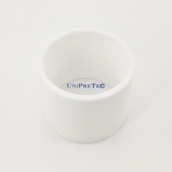
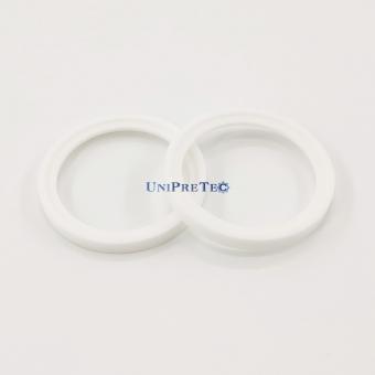
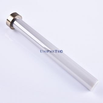
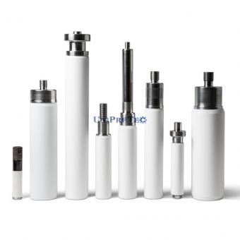
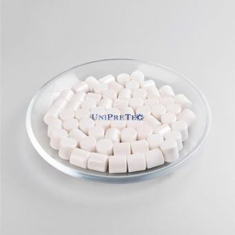
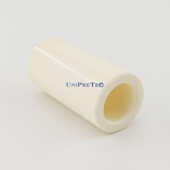
Silicon carbide materials are commonly used in ceramic ball bearings, valves, semiconductor materials, gyroscopes, measuring instruments, aerospace and other fields, and have become an irreplaceable material in many industrial fields.
|
Features
|
|
Physical properties
|
High hardness (Kr's hardness is 3000kg/mm2), can cut ruby.
|
|
High wear resistance, second only to diamond.
|
|
The thermal conductivity is higher than that of copper, 3 times that of Si and 8-10 times that of GaAs.
|
|
SiC has high thermal stability and is impossible to melt under normal pressure.
|
|
Good heat dissipation performance, very important for high-power devices.
|
|
Chemical
properties
|
Very strong corrosion resistance, it can resist almost any known corrosive agent at room temperature.
|
|
The surface of SiC is easy to oxidize to form a thin layer of Si0, which can prevent further oxidation. When it is higher than 1700°C, this oxide film melts and oxidation reaction occurs rapidly.
|
|
The band gap of 4H-SiC and 6H-SC is about 3 times that of Si and 2 times that of GaAs; the breakdown electric field strength is one order of magnitude higher than that of Si, and the saturation electron drift speed is 2.5 times that of Si. 4H-SC has a wider band gap than 6H-SC.
|
2. The physical and chemical properties of silicon carbide
Silicon carbide was first discovered in a meteorite in 1905. Now it is mainly derived from artificial synthesis. Silicon carbide has many uses and a large industry span. It can be used in monocrystalline silicon, polycrystalline silicon, potassium arsenide, quartz crystals, etc., solar photovoltaic industry, Engineering processing materials for the semiconductor industry and piezoelectric crystal industry.
3. Applications in the semiconductor field
Silicon carbide one-dimensional nanomaterials have more unique and excellent properties and broader application prospects due to their own microscopic morphology and crystal structure, and are generally considered to be an important component of the third generation of broadband semiconductor materials.
4. Application in the photovoltaic field
Photovoltaic inverter is very important for photovoltaic power generation. It not only has the function of direct-to-ac conversion, but also has the function of maximizing the performance of solar cells and the function of system failure protection. In summary, there are automatic operation and shutdown functions, maximum power tracking control function, independent operation prevention function (for grid-connected systems), automatic voltage adjustment function (for grid-connected systems), DC detection function (for grid-connected systems), DC grounding detection Function (for grid-connected system), etc.
5. Application in aviation
Silicon carbide is made into silicon carbide fibers, which are mainly used as high temperature resistant materials and reinforcement materials. High temperature resistant materials include heat shielding materials, high temperature resistant conveyor belts, filter cloths for filtering high temperature gases or molten metals, etc. When used as a reinforcing material, it is often used in combination with carbon fiber or glass fiber, mainly reinforced metals (such as aluminum) and ceramics, such as brake pads, engine blades, landing gearboxes and fuselage structural materials for jet aircraft. It can be used as sports goods, and its chopped fiber can be used as high-temperature furnace materials.
6. The development trend of the global semi-insulating silicon carbide wafer material market.
The semi-insulating substrate has high resistance and can withstand higher frequencies, so it has a broad application space in 5G communications and a new generation of intelligent interconnection and sensing devices. The current mainstream semi-insulating substrate products are mainly 4 inches. In 2017, the global market demand for semi-insulating substrates was about 40,000 pieces. It is estimated that by 2020, the market for 4-inch semi-insulating substrates will remain at 40,000, while the market for 6-inch semi-insulating substrates will rapidly increase to 40,000 to 50,000; from 2025 to 2030, 4-inch semi-insulating substrates will gradually withdraw Market, and 6-inch wafers will grow to 200,000 pieces.